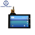
Capacitive touch screen is widely used in industrial equipment as the mainstream technology of the current multi-touch interface, and it is also called industrial touch screen in the industrial control industry. Due to the particularity of the industrial environment, the touch screen is usually required to have anti-electromagnetic interference characteristics, if the anti-interference is weak, it will affect the touch effect of the device, such as insensitive touch, inaccurate and other problems. The electromagnetic interference problem of industrial touch screen is very challenging in the early development.
Projected capacitive touch screen can accurately locate the position of the finger on the screen, it is through the measurement of capacitance of the small changes to identify the finger position. In such touch screen applications, a key design issue to consider is the impact of electromagnetic interference (EMI) on system performance. Performance degradation caused by interference can adversely affect the touch screen design.
Projected Capacitive Touch Screen Architecture
A typical projected capacitive sensor is mounted under a glass or plastic cover. The transmitting (Tx) and receiving (Rx) electrodes are connected to transparent indium tin oxide (ITO) to form a cross-matrix with a characteristic capacitance at each Tx-Rx junction.The Tx ITO is located below the Rx ITO, separated by a layer of polymer film or optical collodion (OCA).
How the sensor works
Let's analyse the operation of a touch screen without considering interference: the operator's finger is at ground potential, the Rx is held at ground potential by the touch screen controller circuitry, and the Tx voltage is variable. The variable Tx voltage causes a current to flow through the Tx-Rx capacitor. A carefully balanced Rx integrated circuit isolates and measures the charge entering the Rx, which represents the "mutual capacitance" connecting the Tx and Rx.
Projected capacitive touchscreens, which are widely used in portable devices today, are susceptible to electromagnetic interference, whereby interfering voltages from internal or external sources are capacitively coupled to the touchscreen device. These interfering voltages can cause charge movement within the touchscreen, which can confuse the measurement of charge movement when a finger touches the screen. The effective design and optimisation of a touch screen system therefore depends on understanding the interference coupling paths and either minimising or compensating for them.
Interference coupling paths involve parasitic effects such as transformer winding capacitance and finger-device capacitance. Proper modelling of these effects allows the source and magnitude of the interference to be fully understood.
For many portable devices, the battery charger constitutes the main source of interference to the touchscreen. When an operator's finger touches the touchscreen, the resulting capacitance allows the charger interference coupling circuit to be closed. The quality of the charger's internal shielding design and the availability of a proper charger grounding design are key factors affecting charger interference coupling.
So how can this problem be solved?
The use of wave-absorbing materials to absorb coupled electromagnetic waves prevents the superposition of waves and eliminates the excess waves present within intelligent electronic systems. Wave-absorbing materials can be cut to shape and affixed to the back of electronic touch panels or to the wiring to combat EMI, as well as to optimise the performance of electronic touch screens.


